Electronic Science - Online Test
Q1. In the ac network shown in the figure, the phasor voltage VA (in Volts) is
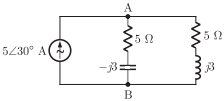
Answer : Option D
Explaination / Solution:
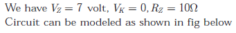
Q2. For the Zener diode shown in the figure, the Zener voltage at knee is 7 V, the
knee current is negligible and the Zener dynamic resistance is 10 Ω. If the input
voltage (Vi) range is from 10 to 16 V, the output voltage (V0) ranges from
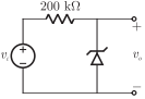
Answer : Option C
Explaination / Solution:
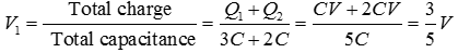
Q3. Two parallel plate capacitors of capacitances C and 2C are connected in parallel and charged to a potential difference V by a battery. The battery is then disconnected and the space between the plates of capacitor C is completely filled with a material of dielectric constant K = 3. The potential difference across the capacitors now becomes
Answer : Option D
Explaination / Solution:
The charges on the capacitors after being charged to a potential V are.After being filled with a material of dielectric K=3 the capacitor which initially had a capacitance C has now the capacitance KC=3C. The common potential
Q4. A silicon PN junction is forward biased with a constant current at room temperature. When the temperature is increased by 10ºC, the forward bias voltage across the PN junction
Answer : Option D
Explaination / Solution:
For every 1º C increase in temperature, forward bias voltage across diode decreases by 2.5 mV. Thus for 10º C increase, there us 25 mV decreases
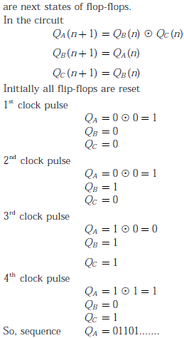
Q5. 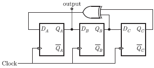
Assuming that the flip-flop are in reset condition initially, the count sequence observed at QA, in the circuit shown is
Answer : Option D
Explaination / Solution:

Q6. In the following graph, the number of trees (P) and the number of cut-set (Q) are
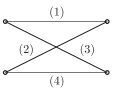
Answer : Option C
Explaination / Solution:
Q7. In the network shown in the figure, C1 = 6 and C = 9 . The equivalent capacitance between points P and Q is
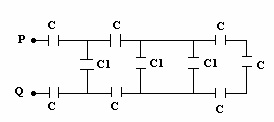
Answer : Option B
Explaination / Solution:
The circuit is reduced as follows: The capacitances are in micro farads.
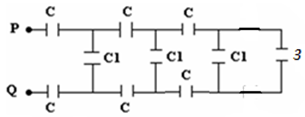
The capacitance between P and Q is 3μF
The capacitance between P and Q is 3μF
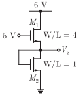
Q8. In the circuit shown below, for the MOS transistors,  and
the threshold voltage VT = 1 V. The voltage Vx at the source of the upper
transistor is
and
the threshold voltage VT = 1 V. The voltage Vx at the source of the upper
transistor is
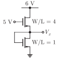
and
the threshold voltage VT = 1 V. The voltage Vx at the source of the upper
transistor is
Answer : Option C
Explaination / Solution:
Given circuit is shown below.
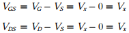
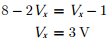
 Thus our assumption is true and Vx = 3 V.
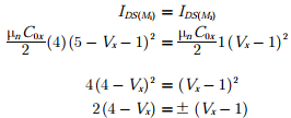
For transistor M2,
Since  thus M2 is in saturation.
By assuming M1 to be in saturation we have
thus M2 is in saturation.
By assuming M1 to be in saturation we have
thus M2 is in saturation.
By assuming M1 to be in saturation we haveTaking positive root,
Thus our assumption is true and Vx = 3 V.
Q9. The Boolean function realized by the logic circuit shown is
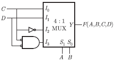
Answer : Option D
Explaination / Solution:
Output of the MUX can be written as
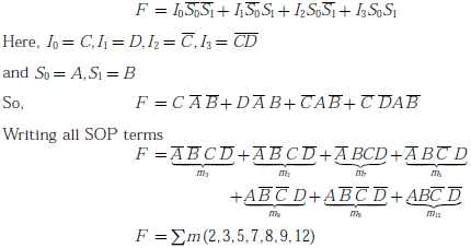
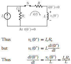
Q10. In the following circuit, the switch S is closed at t = 0. The rate of change of
current  is given by
Answer : Option B
Explaination / Solution:
Initially i(0-) = 0 therefore due to inductor i(0+) = 0. Thus all current Is will
flow Is in resistor R and voltage across resistor will be IsRs. The voltage across
inductor will be equal to voltage across Rs as no current flow through R.