EC GATE 2007 - Online Test
Q1. If R(τ) is the auto correlation function of a real, wide-sense stationary random process, then which of the following is NOT true
Answer : Option C
Explaination / Solution:
No Explaination.
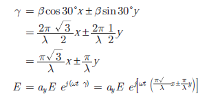
Q2. A plane wave of wavelength λ is traveling in a direction making an angle 300 with positive x − axis and 900 with positive y − axis. The  field of the plane
wave can be represented as (E is constant)
field of the plane
wave can be represented as (E is constant)
Answer : Option A
Explaination / Solution:
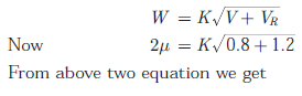
Q3. A p n junction has a built-in potential of 0.8 V. The depletion layer width a
reverse bias of 1.2 V is 2 μm. For a reverse bias of 7.2 V, the depletion layer
width will be
Answer : Option A
Explaination / Solution:
Q4. If S(f) is the power spectral density of a real, wide-sense stationary random process, then which of the following is ALWAYS true?
Answer : Option B
Explaination / Solution:
No Explaination.
Q5. Group I lists four types of p − n junction diodes. Match each device in Group I with one of the option in Group II to indicate the bias condition of the device in its normal mode of operation.
Group - I Group-II
(P) Zener Diode (1) Forward bias
(Q) Solar cell (2) Reverse bias
(R) LASER diode
(S) Avalanche Photodiode
Answer : Option B
Explaination / Solution:
Zener diode and Avalanche diode works in the reverse bias and laser diode works in forward bias.
In solar cell diode works in forward bias but photo current is in reverse direction. Thus
Zener diode : Reverse Bias
Solar Cell : Forward Bias
Laser Diode : Forward Bias
Avalanche Photo diode : Reverse Bias
Q6. In delta modulation, the slope overload distortion can be reduced by
Answer : Option D
Explaination / Solution:
No Explaination.
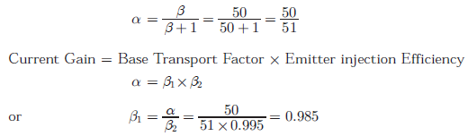
Q7. The DC current gain (β) of a BJT is 50. Assuming that the emitter injection
efficiency is 0.995, the base transport factor is
Answer : Option B
Explaination / Solution:
Q8.
Group I lists four different semiconductor devices. match each device in Group I with its charactecteristic property in Group II
Group-I Group-II
(P) BJT (1) Population iniversion
(Q) MOS capacitor (2) Pinch-off voltage
(R) LASER diode (3) Early effect
(S) JFET (4) Flat-band voltage
Answer : Option C
Explaination / Solution:
In BJT as the B-C reverse bias voltage increases, the B-C space charge region
width increases which xB (i.e. neutral base width) > A change in neutral base
width will change the collector current. A reduction in base width will causes
the gradient in minority carrier concentration to increase, which in turn causes
an increased in the diffusion current. This effect si known as base modulation as
early effect.
In JFET the gate to source voltage that must be applied to achieve pinch off
voltage is described as pinch off voltage and is also called as turn voltage or
threshold voltage.
In LASER population inversion occurs on the condition when concentration of
electrons in one energy state is greater than that in lower energy state, i.e. a non
equilibrium condition.
In MOS capacitor, flat band voltage is the gate voltage that must be applied to
create flat ban condition in which there is no space charge region in semiconductor
under oxide.
Therefore
BJT : Early effect
MOS capacitor : Flat-band voltage
LASER diode : Population inversion
JFET : Pinch-off voltage
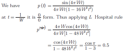
Q9. The raised cosine pulse p(t) is used for zero ISI in digital communications. The
expression for p(t) with unity roll-off factor is given by
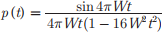
The value of p(t) at t = 1/W is
Answer : Option C
Explaination / Solution:
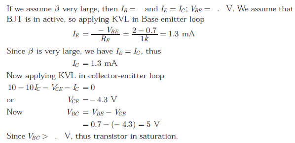
Q10. For the BJT circuit shown, assume that the β of the transistor is very large and VBE = . V. The mode of operation of the BJT is
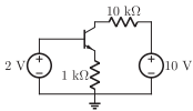
Answer : Option B
Explaination / Solution: