Electronic Science - Online Test
Q1. In the circuit shown below, capacitors C1 and C2 are very large and are shorts
at the input frequency. vi is a small signal input. The gain magnitude  at 10
M rad/s is
at 10
M rad/s is
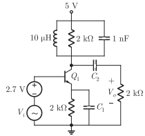
Answer : Option A
Explaination / Solution:
For the parallel RLC circuit resonance frequency is,
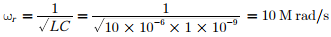

 which is maximum
Thus given frequency is resonance frequency and parallel RLC circuit has
maximum impedance at resonance frequency
Gain of the amplifier is  where ZC is impedance of parallel RLC
circuit.
where ZC is impedance of parallel RLC
circuit.
where ZC is impedance of parallel RLC
circuit.Hence at this frequency (ωr), gain is
which is maximumTherefore gain is maximum at ωr = 10 /sec M rad .
Q2. Match the logic gates in Column A with their equivalents in Column B
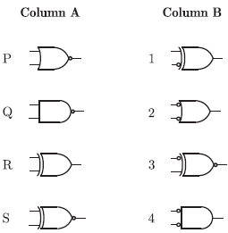
Answer : Option D
Explaination / Solution:
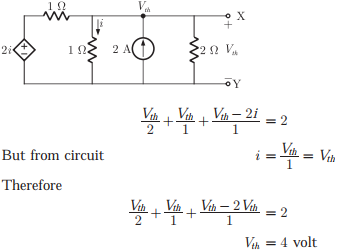
Q3. 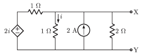
For the circuit shown in the figure, the Thevenin voltage and resistance looking into X − Y are
Answer : Option D
Explaination / Solution:
Here Vth is voltage across node also. Applying nodal analysis we get
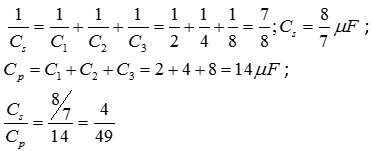
Q4. Three condensers of capacity 2 μF , 4 μF and 8 μF respectively, are first connected in series and then connected in parallel. The ratio of the equivalent capacitance in the two cases will be
Answer : Option D
Explaination / Solution:
Q5. Drift current in the semiconductors depends upon
Answer : Option C
Explaination / Solution:
No Explaination.
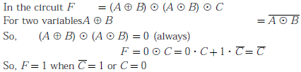
Q6. 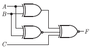
For the output F to be 1 in the logic circuit shown, the input combination should be
Answer : Option C
Explaination / Solution:
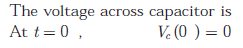
Q7. In the circuit shown, vC is 0 volts at t = 0 sec. For t > 0, the capacitor current iC(t), where t is in seconds is given by
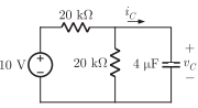
Answer : Option A
Explaination / Solution:
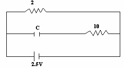
Q8. A capacitor of capacitance C = 2 is connected as shown in the figure. If the internal resistance of the cell is 0.5, the charge on the capacitor plates is
Answer : Option C
Explaination / Solution:
At steady state no current flows through the capacitor. The total resistance in the circuit =2+0.5=2.5Ω. Current I=V/R=2.5/2.5=1A. since no current flows through the 10 Ω resistor, the potential drop across it =0. The potential drop across the 2 Ω resistor = potential across the capacitor= I×2=2V.Charge on the capacitor Q= CV=(2μF)×(2V)=4μC.
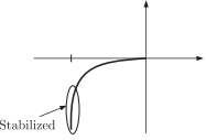
Q9. A Zener diode, when used in voltage stabilization circuits, is biased in
Answer : Option B
Explaination / Solution:
Zener diode operates in reverse breakdown region.
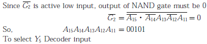
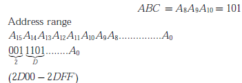
Q10. In the circuit shown, the device connected Y5 can have address in the range

Answer : Option B
Explaination / Solution: