Electronic Science - Online Test
Q1. In the circuit shown below, the knee current of the ideal Zener dioide is 10 mA
. To maintain 5 V across RL, the minimum value of RL in Ω and the minimum
power rating of the Zener diode in mW, respectively, are
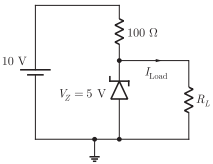
Answer : Option B
Explaination / Solution:
No Explaination.
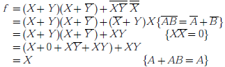
Q2. If X = 1 in logic equation  Then
Then
Then
Answer : Option D
Explaination / Solution:

Substituting X = 1 and we get
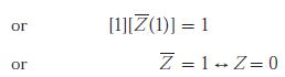 1 + A = 1 and 0 + A = A
Substituting X = 1 and
1 + A = 1 and 0 + A = A
Q3. In the circuit shown, the power supplied by the voltage source is
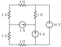
Answer : Option A
Explaination / Solution:
Applying nodal analysis
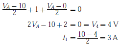
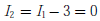
Current from voltage source is
Since current through voltage source is zero, therefore power delivered is zero.
Q4. The small-signal resistance  in kW offered by the n-channel
MOSFET M shown in the figure below, at a bias point of VB = 2V is (device
data for M: device transconductance parameter
in kW offered by the n-channel
MOSFET M shown in the figure below, at a bias point of VB = 2V is (device
data for M: device transconductance parameter 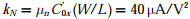 , threshold voltage VTN = 1V, and neglect body effect and channel length
modulation effects)
, threshold voltage VTN = 1V, and neglect body effect and channel length
modulation effects)
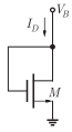
in kW offered by the n-channel
MOSFET M shown in the figure below, at a bias point of VB = 2V is (device
data for M: device transconductance parameter , threshold voltage VTN = 1V, and neglect body effect and channel length
modulation effects)
Answer : Option A
Explaination / Solution:
No Explaination.
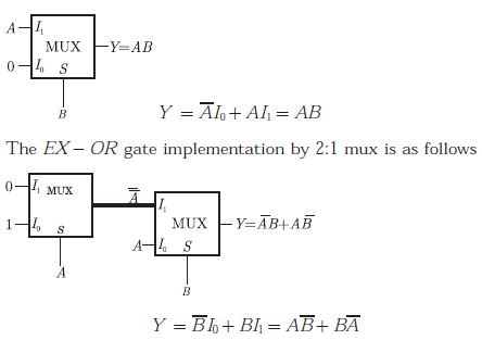
Q5. What are the minimum number of 2- to -1 multiplexers required to generate a 2- input AND gate and a 2- input Ex-OR gate
Answer : Option A
Explaination / Solution:
The AND gate implementation by 2:1 mux is as follows
Q6. 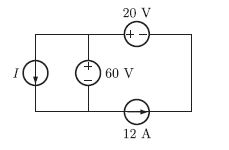
In the interconnection of ideal sources shown in the figure, it is known that the 60 V source is absorbing power.
Which of the following can be the value of the current source I ?
Answer : Option A
Explaination / Solution:
Circuit is as shown below
Since 60 V source is absorbing power. So, in 60 V source current flows from + to - ve direction So,
I + I1 = 12
I = 12 - I1
I is always less then 12 A So, only option (A) satisfies this conditions.
Q7. The ac schematic of an NMOS common-source state is shown in the figure
below, where part of the biasing circuits has been omitted for simplicity. For the
n-channel MOSFET M, the transconductance  and body effect
and channel length modulation effect are to be neglected. The lower cutoff
frequency in HZ of the circuit is approximately at
and body effect
and channel length modulation effect are to be neglected. The lower cutoff
frequency in HZ of the circuit is approximately at
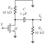
and body effect
and channel length modulation effect are to be neglected. The lower cutoff
frequency in HZ of the circuit is approximately at
Answer : Option A
Explaination / Solution:
No Explaination.
Q8. The Boolean expression 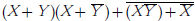 simplifies to
simplifies to
Answer : Option C
Explaination / Solution:
Given the Boolean expression

We simplify the expression as
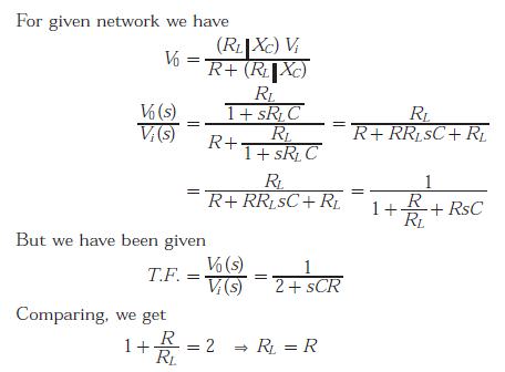
Q9. If the transfer function of the following network is
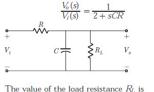
Answer : Option C
Explaination / Solution:
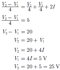
Q10. In the given circuit, the values of V1 and V2 respectively are
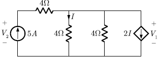
Answer : Option A
Explaination / Solution:
By Nodal analysis