Electronic Science - Online Test
Q1. 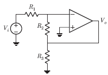
Assuming the OP-AMP to be ideal, the voltage gain of the amplifier shown below is
Answer : Option A
Explaination / Solution:
Q2. 
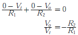
Figure shows a composite switch consisting of a power transistor (BJT) in series with a diode. Assuming that the transistor switch and the diode are ideal , the I-V characteristic of the composite switch is
Answer : Option C
Explaination / Solution:
No Explaination.
Q3. The impurity atoms with which pure silicon should be doped to make a p-type semiconductor are those of
Answer : Option A
Explaination / Solution:
In a pure (intrinsic) Si or Ge semiconductor, each nucleus uses its four valence electrons to form four covalent bonds with its neighbors . Each ionic core, consisting of the nucleus and non-valent electrons, has a net charge of +4, and is surrounded by 4 valence electrons. Since there are no excess electrons or holes In this case, the number of electrons and holes present at any given time will always be equal. Note each +4 ion is surrounded by four electrons.
Now, if one of the atoms in the semiconductor lattice is replaced by an element with three valence electrons, such as a Group 3 element like Boron (B) or Gallium (Ga), the electron-hole balance will be changed.
This impurity will only be able to contribute three valence electrons to the lattice, therefore leaving one excess hole . Since holes will "accept" free electrons, a Group 3 impurity is also called an acceptor.
A semiconductor doped with an acceptor. An excess hole is now present. Because an acceptor donates excess holes, which are considered to be positively charged, a semiconductor that has been doped with an acceptor is called a p-type semiconductor.
Q4. In the sequential circuit shown below, if the initial value of the output Q1Q0 is 00,
what are the next four values of Q1Q0?
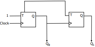
Answer : Option D
Explaination / Solution:
No Explaination.
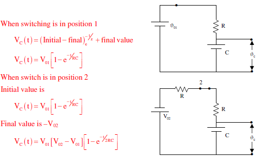
Q5. The switch SW shown in the circuit is kept at position ‘1’ for a long duration.
At
t
= 0+, the switch is moved to position ‘2’. Assuming |Vo2| > |Vo1|, the voltage vc(t) across the capacitor is
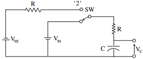
Answer : Option D
Explaination / Solution:
Q6. If the dielectric constant and dielectric strength be denoted by K and X respectively, then a material suitable for use as a dielectric in a capacitor must have
Answer : Option D
Explaination / Solution:
The capacitance of a capacitor increases with increase in the value of dielectric constant. =K C. Dielectric strength is the maximum electric field the material can withstand without breaking down. A high value of X and a high value of K is preferable for use in capacitors.
Q7. The magnetic field due to very long wire carrying current varies according to
Answer : Option C
Explaination / Solution:
The magnetic field at a point, which is at a distance r, from a very long wire carrying current is
Q8. The logical gate implemented using the circuit shown below where. V1 and V2 are inputs (with
0 V as digital 0 and 5 V as digital 1) and Vout is the output is
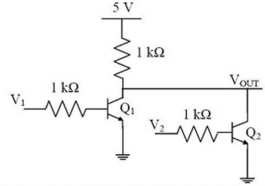
Answer : Option B
Explaination / Solution:
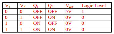
So, this logic level o/p is showing the functionality of NOR-gate.
Q9. A capacitor is charged and then made to discharge through a resistance. The time constant is τ. In what time will the potential difference across the capacitor decreases by 10%?
Answer : Option D
Explaination / Solution:
The capacitance of a capacitor is a constant.
Also, V q
The discharging equation for capacitor is
A similar equation can be written for potential difference.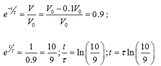
Q10. If the area under the B-H curve of a material M is more, in an ac solenoid using material M
Answer : Option A
Explaination / Solution:
No Explaination.
