Electronic Science - Online Test
Q1. 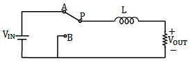
The power electronic converter shown in the figure has a single-pole double-throw switch. The pole P of the switch is connected alternately to throws A and B. The converter shown is a _______
Answer : Option A
Explaination / Solution:
No Explaination.
Q2. To obtain a p-type germanium semiconductor, it must be doped with
Answer : Option C
Explaination / Solution:
p-type germanium semiconductor is formed when it is doped with a trivalent impurity atom. So it should be doped with indium.
Q3. In the circuit shown below, the knee current of the ideal Zener diode is 10 mA. To maintain 5 V
across RL, the minimum value of RL in Ω and the minimum power rating of the Zener diode in mW
respectively are
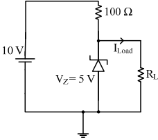
Answer : Option B
Explaination / Solution:
No Explaination.
Q4. What is the Boolean expression for the output f of the combinational logic circuit
of NOR gates given below?
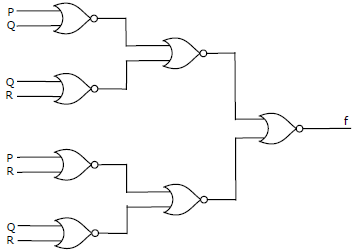
Answer : Option B
Explaination / Solution:
No Explaination.
Q5. The dielectric constant K of an insulator cannot be
Answer : Option A
Explaination / Solution:
Dielectric constant of a metal is infinity, and this is why the electric field inside a metal is zero. All other substances have a dielectric constant with values less than infinity but greater than 1.
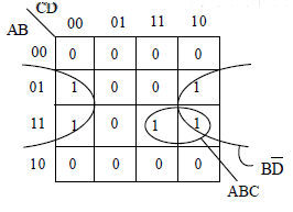
Q6. The output expression for the Karnaugh map shown below is
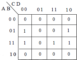
Answer : Option D
Explaination / Solution:
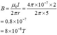
Q7. A long straight wire carries an electric current of 2 A. The magnetic induction at a perpendicular distance of 5 m from the wire is
()
Answer : Option B
Explaination / Solution:
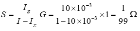
Q8. A milliammeter of range 10 mA has a coil of resistance 1 Ω.To use it as an ammeter of range 1 A, the required shunt must have a resistance of
Answer : Option C
Explaination / Solution:
(Theory in chapter 4 – magnetic effect of current)
(Theory in chapter 4 – magnetic effect of current)
Q9. To increase the magnetic field of a solenoid what core material should be used ?
Answer : Option A
Explaination / Solution:
No Explaination.
Q10. At room temperature, a possible value for the mobility of electrons in the inversion layer of a silicon n-channel MOSFET is
Answer : Option A
Explaination / Solution:
At room temperature mobility of electrons for Si sample is given μn = 1350 cm2/V-s For an n-channel MOSFET to create an inversion layer of electrons, a large positive gate voltage is to be applied. Therefore, induced electric field increases and mobility decreases.
So, Mobility μn <1350 cm2/V-s for n-channel MOSFET
