Electronic Science - Online Test
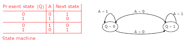
Q1. The state transition diagram for the logic circuit shown is
Answer : Option D
Explaination / Solution:
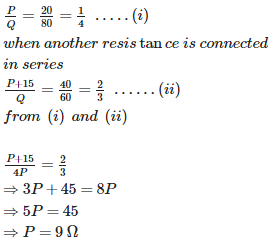
Q2. Two resistances are connected in the two gaps of a meter bridge. The balance points is 20 cm from the zero end. When a resistance of 15 ohm is connected in series with the smaller of the two resistances, the null point shifts to 40 cm. The smaller of the two resistances has the value (in ohm)
Answer : Option A
Explaination / Solution:
Let the resistances be P and Q. When balanced,
Q3. magnetic potential energy Um of Compass needle of known magnetic moment m in a uniform magnetic field field is
Answer : Option D
Explaination / Solution:
No Explaination.
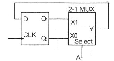
Q4. Consider the following circuit involving three D-type flip-flops used in a certain
type of counter configuration.
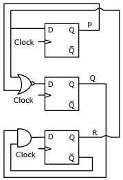
If all the flip-flops were reset to 0 at power on, what is the total number of
distinct outputs (states) represented by PQR generated by the counter?
Answer : Option C
Explaination / Solution:
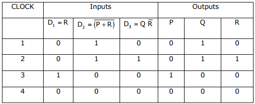
So Total number of distinct outputs is 4
Q5. Three moving iron type voltmeters are connected as shown below. Voltmeter
readings are V, V1 and V2 as indicated. The correct relation among the voltmeter
readings is
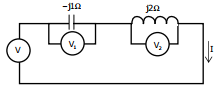
Answer : Option B
Explaination / Solution:
No Explaination.
Q6. The total current in a semiconductor is
Answer : Option B
Explaination / Solution:
Electrons will experience a attractive force from the positive terminal, so they move towards the positive terminal of the battery by carrying the electric current.
Similarly holes will experience a attractive force from the negative terminal, so they moves towards the negative terminal of the battery by carrying the electric current.
Thus, in a semiconductor electric current is carried by both electrons and holes. In intrinsic semiconductor the number of free electrons in conduction band is equal to the number of holes in valence band.
The current caused by electrons and holes is equal in magnitude. The total current in intrinsic semiconductor is the sum of hole and electron current.
Total current = Electron current + Hole current I =
Q7. The unit of potential difference as used in electrical circuits is
Answer : Option D
Explaination / Solution:
Volt is the unit of potential difference.
Q8.
The figure shows the high-frequency capacitance - voltage characteristics of Metal/Sio2/silicon (MOS) capacitor having an area of 1 × 10⁻⁴ cm2. Assume that the permittivities (ε0εr) of silicon and Sio are 1 × 10-12 F/cm and 3.5 × 10⁻¹³ F/ cm respectively.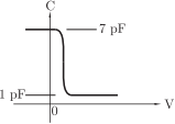
Consider the following statements about the C − V characteristics plot :
S1 : The MOS capacitor has as n-type substrate
S2 : If positive charges are introduced in the oxide, the C − V polt will shift to the left.
Then which of the following is true?
Answer : Option C
Explaination / Solution:
Depletion region will not be formed if the MOS capacitor has n type substrate but from C-V characteristics, C reduces if V is increased. Thus depletion region must be formed. Hence S1 is false
If positive charges is introduced in the oxide layer, then to equalize the effect the applied voltage V must be reduced. Thus the C − V plot moves to the left. Hence S2 is true.
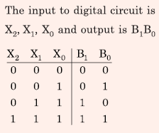
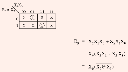
Q9. A 2-bit flash Analog to Digital Converter (ADC) is given below. The input is 0 ≤ VIN ≤ 3 Volts.
The expression for the LSB of the output B0 as a Boolean function of X2, X1, and X0 is
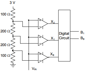
Answer : Option A
Explaination / Solution:
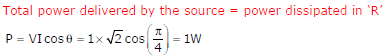
Q10. An RLC circuit with relevant data is given below.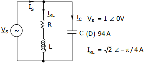
The power dissipated in the resistor R is
Answer : Option B
Explaination / Solution: