Electronics Engineering - Online Test
Q1. Consider an angle modulated signal  The average power of x(t) is
The average power of x(t) is
Answer : Option B
Explaination / Solution:
No Explaination.
Q2. A good transconductance amplifier should have
Answer : Option C
Explaination / Solution:
A good trans conductance amplifier should have high input and output resistance.
Q3. In the following circuit, X is given by
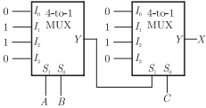
Answer : Option A
Explaination / Solution:
Q4. A region of negative differential resistance is observed in the current voltage characteristics of a silicon PN junction if
Answer : Option A
Explaination / Solution:
In case of Tunnel diode formed by PN junction, tunnel diode gives negative resistance and works in forward bias, and in tunnel diode both N and P regions are heavily doped.
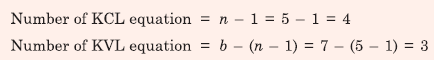
Q5. The graph associated with an electrical network has 7 branches and 5 nodes. The number of independent KCL equations and the number of independent KVL equations, respectively, are
Answer : Option D
Explaination / Solution:
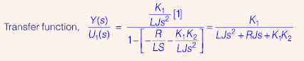
Q6. In the system whose signal flow graph is shown in the figure, U1(s) and U2(s) are inputs. The
transfer function Y(s)/U1(s) is
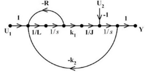
Answer : Option A
Explaination / Solution:
Q7. At t = 0, the function f(t) = sint/t has
Answer : Option B
Explaination / Solution:
No Explaination.
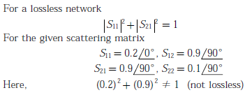
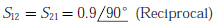
Q8. If the scattering matrix [S ] of a two port network is 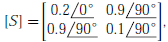 then the network is
then the network is
Answer : Option C
Explaination / Solution:
Q9. The following binary values were applied to the X and Y inputs of NAND latch
shown in the figure in the sequence indicated below : 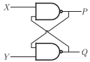
X = ,Y = X = ,Y = X = Y =
The corresponding stable P Q, output will be
Answer : Option C
Explaination / Solution:
No Explaination.
Q10. For the circuit with ideal diodes shown in the figure, the shape of the output (Vout) for the given sine wave input (Vin) will be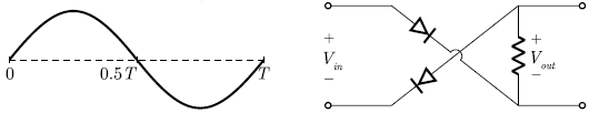
Answer : Option C
Explaination / Solution:
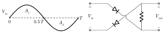
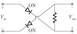
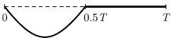
For positive half A1, we have
Vout = - Vin
For negative half A2, both diode will be OFF.
So, Vout = 0
Hence, the output is obtained as
