Electronic Science - Online Test
Q1.
Estimate the output voltage V0 for VG = 1.5 V. [Hints : Use the appropriate current-voltage equation for each MOSFET, based on the answer to Q.57]
Answer : Option C
Explaination / Solution:
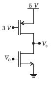
Consider for CMOS circuit shown, where the gate voltage v0 of the n-MOSFET is increased from zero, while the gate voltage of the p -MOSFET is kept constant at 3 V. Assume, that, for both transistors, the magnitude of the threshold voltage is 1 V and the product of the trans-conductance parameter is 1mA. V-2
Q2. 
For each of the positive edge-triggered J - K flip flop used in the following figure, the propagation delay is Δt .
Which of the following wave forms correctly represents the output at Q1?
Answer : Option B
Explaination / Solution:
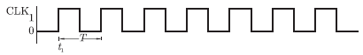
Since the input to both JK flip-flop is 11, the output will change every time with clock pulse. The input to clock is
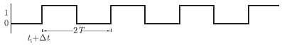
The output Q0 of first FF occurs after time ΔT and it is as shown below
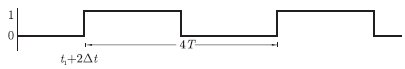
The output Q1 of second FF occurs after time ΔT when it gets input (i.e. after ΔT from t1) and it is as shown below
Q3. A short bar magnet has a magnetic moment of 0.48 J/T .Magnetic field produced by the magnet at a distance of 10 cm from the centre of the magnet on the axis has a direction and magnitude of .
Answer : Option B
Explaination / Solution:
No Explaination.
Q4. When we apply reverse bias to a junction diode it
Answer : Option C
Explaination / Solution:
When a diode is connected in a Reverse Bias condition, a positive voltage is applied to the N-type material and a negative voltage is applied to the P-type material.
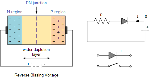
The positive voltage applied to the N-type material attracts electrons towards the positive electrode and away from the junction, while the holes in the P-type end are also attracted away from the junction towards the negative electrode.
The net result is that the depletion layer grows wider due to a lack of electrons and holes and presents a high impedance path, almost an insulator. The result is that a high potential barrier is created thus preventing current from flowing through the semiconductor material
Q5. A wire of given length is first bent in one loop and then in three loops. If same current is passed in both cases, the ratio of magnetic inductions at the centre will be
Answer : Option C
Explaination / Solution:
1 : 9
Q6. The current through the 2 kΩ resistance in the circuit shown is

Answer : Option A
Explaination / Solution:
It is a balanced Wheatstone bridge.
Q7. If the charge on a capacitor is increased by 2 coulomb, the energy stored in it increases by 21%. The original charge on the capacitor (in coulomb) is
Answer : Option B
Explaination / Solution:
The initial energy of the capacitor of capacitance C and charge Q1 is .When the charge increases to Q2 the energy of the capacitor Given percentage increase of energy
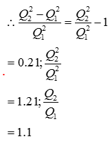
. But Solving
. But Solving
Q8. 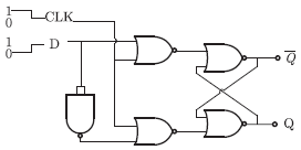
For the circuit shown in the figure, D has a transition from 0 to 1 after CLK changes from 1 to 0. Assume gate delays to be negligible. Which of the following statements is true
Answer : Option A
Explaination / Solution:
No Explaination.
Q9. In a forward biased pn junction diode, the sequence of events that best describes the mechanism of current flow is
Answer : Option A
Explaination / Solution:
The potential barrier of the pn junction is lowered when a forward bias voltage is applied, allowing electrons and holes to flow across the space charge region (Injection) when holes flow from the p region across the space charge region into the n region, they become excess minority carrier holes and are subject to diffuse, drift and recombination processes.
Hence correct option is (A)
Q10. A closely wound solenoid of 2000 turns and area of cross-section , carrying a current of 4.0 A, is suspended through its centre allowing it to turn in a horizontal plane. If a uniform horizontal magnetic field of T is set up at an angle of with the axis of the solenoid,force and torque on the solenoid are
Answer : Option A
Explaination / Solution:
No Explaination.
