Electronic Science - Online Test
Q1. For the Op-Amp circuit shown in the figure, V is
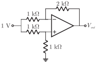
Answer : Option C
Explaination / Solution:
No Explaination.
Q2. Which of the following is true about equipotential lines
Answer : Option B
Explaination / Solution:
The potential at all points on an equipotential surface is constant and work done in moving a charge on an equipotential surface is zero. Electric field lines show the direction of the electric field at the point. If the electric field lines were tangential, parallel or opposite to the equipotential surface, a tangential field will exist on the surface and work done in moving a charge on the surface is not zero. Therefore electric field lines are always perpendicular to the equipotential surface.
Q3. For two parallel wires carrying currents Ia and Ib seperated by a distance d, the magnitude of force acting on length L of any of the wires is
Answer : Option B
Explaination / Solution:
The conductor carrying current Ib is placed in the magnetic field created by the conductor carrying current . The force it experiences
Q4.
The measured trans conductance gm of an NMOS transistor operating in the linear region is plotted against the gate voltage VG at a constant drain voltage VD. Which of the following figures represents the expected dependence of gm on VG ?
Answer : Option C
Explaination / Solution:
No Explaination.
Q5. A current is passed though two coils connected in series. The potential difference across the first coil of resistance 2 ohm is 5 volt. If the potential difference across the second coil is 12.5 volt the resistance of the second coil is
Answer : Option A
Explaination / Solution:
The current in the circuit
V1 =5 V is the p.d across the first coil of resistance R1=2Ω. The same current flows through the second coil of resistance X. . The p.d across the second coil V2 =12.5 V.
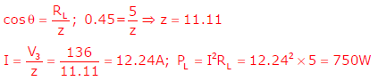
Q6. In the circuit shown, the three voltmeter readings are V1 = 220 V , V2 = 122 V, V3 = 136 V .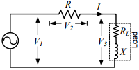
If RL = 5Ω , the approximate power consumption in the load is
Answer : Option B
Explaination / Solution:
Q7. Magnetic material differences are explained by
Answer : Option D
Explaination / Solution:
No Explaination.
Q8. A wattmeter is connected as shown in the figure. The wattmeter reads
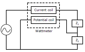
Answer : Option D
Explaination / Solution:
No Explaination.
Q9. Depletion region (space charge) is formed because
Answer : Option C
Explaination / Solution:
The depletion region, also called depletion layer, depletion zone, junction region, space charge region or space charge layer, is an insulating region within a conductive, doped semiconductor material where the mobile charge carriers have been diffused away, or have been forced away by an electric field. The only elements left in the depletion region are ionized donor or acceptor impurities.
The depletion region is so named because it is formed from a conducting region by removal of all free charge carriers, leaving none to carry a current.
Q10. Which one of the following is NOT logically equivalent to ¬∃x (∀y (α) ∧ ∀z (β))?
Answer : Option A
Explaination / Solution:
No Explaination.
