Electronics Engineering - Online Test
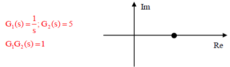
Q1. Nyquist plot of two functions G1(s) and G2(s) are shown in figure.
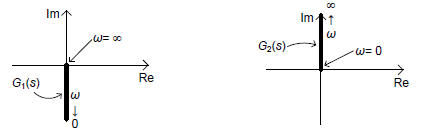
Nyquist plot of the product of G1(s) and G2(s) is
Answer : Option B
Explaination / Solution:
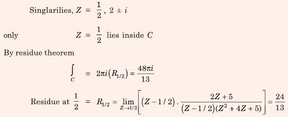
Q2. The value of the integral
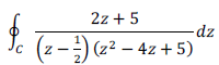
over the contour |z| = 1, taken in the anti-clockwise direction, would be
Answer : Option B
Explaination / Solution:
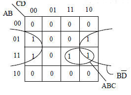
Q3. The output expression for the Karnaugh map shown below is
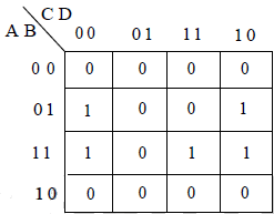
Answer : Option D
Explaination / Solution:
Q4. In the design of a single mode step index optical fibre close to upper cut-off, the single-mode operation is not preserved if
Answer : Option C
Explaination / Solution:
No Explaination.
Q5. At room temperature, a possible value for the mobility of electrons in the inversion layer of a silicon n-channel MOSFET is
Answer : Option A
Explaination / Solution:
At room temperature mobility of electrons for Si sample is given μn = 1350 cm2/V-s For an n-channel MOSFET to create an inversion layer of electrons, a large positive gate voltage is to be applied. Therefore, induced electric field increases and mobility decreases.
So, Mobility μn <1350 cm2/V-s for n-channel MOSFET
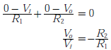
Q6. 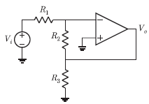
Assuming the OP-AMP to be ideal, the voltage gain of the amplifier shown below is
Answer : Option A
Explaination / Solution:
Q7. 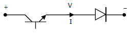
Figure shows a composite switch consisting of a power transistor (BJT) in series with a diode. Assuming that the transistor switch and the diode are ideal , the I-V characteristic of the composite switch is
Answer : Option C
Explaination / Solution:
No Explaination.
Q8. In the sequential circuit shown below, if the initial value of the output Q1Q0 is 00,
what are the next four values of Q1Q0?
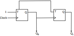
Answer : Option D
Explaination / Solution:
No Explaination.
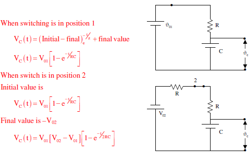
Q9. The switch SW shown in the circuit is kept at position ‘1’ for a long duration.
At
t
= 0+, the switch is moved to position ‘2’. Assuming |Vo2| > |Vo1|, the voltage vc(t) across the capacitor is
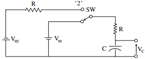
Answer : Option D
Explaination / Solution:
Q10. 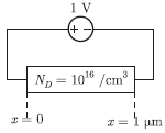
The silicon sample with unit cross-sectional area shown below is in thermal equilibrium. The following information is given: T = 300 K electronic charge = 1.6 × 10⁻¹⁹ C, thermal voltage = 26 mV and electron mobility = 1350 cm2 / V-s
The magnitude of the electric field at x = 0.5 μm is
Answer : Option C
Explaination / Solution:
No Explaination.
