Electrical Engineering - Online Test
Q1. The L-C circuit shown in the figure has an inductance L = 1mH and a capacitance C = 10µF. 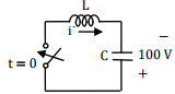
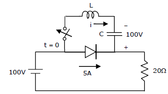
The L – C circuit of Q.9 is used to commutate a thyristor. Which is initially carrying a current of 5 A as shown in the figure below. The values and initial conditions of L and C are the same as in Q.9. The switch is closed at t=0. If the forward drop is negligible, the time taken for the device to turn off is
Answer : Option A
Explaination / Solution:
No Explaination.
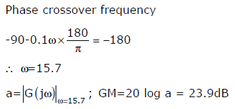
Q2. The open loop transfer function of a unity feedback system is given by  The gain margin of this system is
The gain margin of this system is
Answer : Option D
Explaination / Solution:
Q3. An independent voltage source in series with an impedance Zs = Rs + jXs delivers a maximum average power to a load impedance ZL when
Answer : Option D
Explaination / Solution:
According to maximum Power Transform Theorem
ZL = Zs = (Rs - jXs)
Q4. Consider a wireless communication link between a transmitter and a receiver located in free space, with finite and strictly positive capacity. If the effective areas of the transmitter and the receiver antennas, and the distance between them are all doubled, and everything else remains unchanged, the maximum capacity of the wireless link
Answer : Option C
Explaination / Solution:

Channelcpacity remain same.
Q5. A Hilbert transformer is a
Answer : Option A
Explaination / Solution:
No Explaination.
Q6.
Estimate the output voltage V0 for VG = 1.5 V. [Hints : Use the appropriate current-voltage equation for each MOSFET, based on the answer to Q.57]
Answer : Option C
Explaination / Solution:
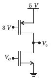
Consider for CMOS circuit shown, where the gate voltage v0 of the n-MOSFET is increased from zero, while the gate voltage of the p -MOSFET is kept constant at 3 V. Assume, that, for both transistors, the magnitude of the threshold voltage is 1 V and the product of the trans-conductance parameter is 1mA. V-2
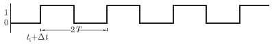
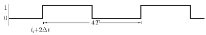
Q7. 
For each of the positive edge-triggered J - K flip flop used in the following figure, the propagation delay is Δt .
Which of the following wave forms correctly represents the output at Q1?
Answer : Option B
Explaination / Solution:
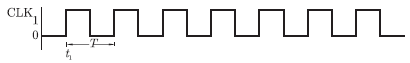
Since the input to both JK flip-flop is 11, the output will change every time with clock pulse. The input to clock is
The output Q0 of first FF occurs after time ΔT and it is as shown below
The output Q1 of second FF occurs after time ΔT when it gets input (i.e. after ΔT from t1) and it is as shown below
Q8. The value of the quantity P, where  is equal to
is equal to
Answer : Option B
Explaination / Solution:
No Explaination.
Q9. The current through the 2 kΩ resistance in the circuit shown is

Answer : Option A
Explaination / Solution:
It is a balanced Wheatstone bridge.
Q10. If the closed-loop transfer function of a control system is given as 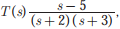 then It is
then It is
Answer : Option D
Explaination / Solution:
In a minimum phase system, all the poles as well as zeros are on the left half of the s −plane. In given system as there is right half zero (s = 5), the system is a non-minimum phase system.
