Electrical Engineering - Online Test
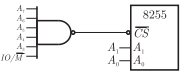
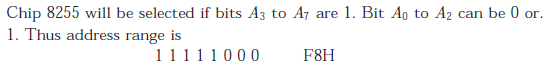
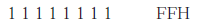
Q1. An 8255 chip is interfaced to an 8085 microprocessor system as an I/O mapped
I/O as show in the figure. The address lines A0 and A1 of the 8085 are used
by the 8255 chip to decode internally its thee ports and the Control register.
The address lines A3 to A as well as the  signal are used for address
decoding. The range of addresses for which the 8255 chip would get selected is
signal are used for address
decoding. The range of addresses for which the 8255 chip would get selected is
Answer : Option C
Explaination / Solution:
Q2.
Consider the following two statements about the internal conditions in a n - channel MOSFET operating in the active region.
S1 : The inversion charge decreases from source to drain
S2 : The channel potential increases from source to drain.
Which of the following is correct?
Answer : Option D
Explaination / Solution:
Both S1 and S2 are true and S2 is a reason for S1.
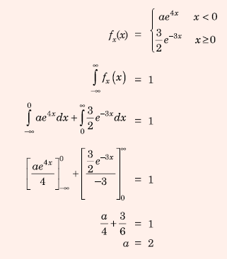
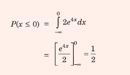
Q3. 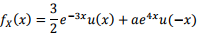
Let the probability density function of a random variable, X, be given as:
where u(x) is the unit step function.
Then the value of 'a' and Prob {X ≤ 0}, respectively, are
Answer : Option A
Explaination / Solution:
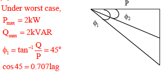
Q4. A load is supplied by a 230 V, 50 Hz source. The active power P and the reactive power Q consumed by the load are such that 1 kW ≤ P ≤ 2kW and 1kVAR ≤ Q ≤ kVAR . A capacitor connected across the load for power factor correction generates 1 kVAR reactive power. The worst case power factor after power factor correction is
Answer : Option B
Explaination / Solution:
Q5. The frequency response of G(s) = 1/[s(s + 1)(s + 2)] plotted in the complex G(jω) plane (for 0 < ω < ∞) is
Answer : Option A
Explaination / Solution:
No Explaination.
Q6. The system ẋ = Ax + Bu with 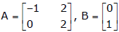 is
is
is
Answer : Option C
Explaination / Solution:
No Explaination.
Q7. For the power system shown in the figure below, the specifications of the components are the
following: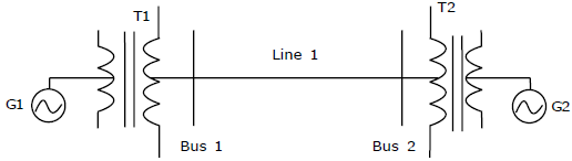
G1 : 25 kV, 100 MVA, X = 9%
G2: 25 kV, 100 MVA, X = 9%
T1: 25 kV/220 kV, 90 MVA, X = 12%
T2: 220 kV/25 kV, 90 MVA, X = 12%
Line 1: 220 kV, X = 150 ohms
Choose 25kV as the base voltage at the generator G1, and 200 MVA as the MVA base. The
impedance diagram is
Answer : Option B
Explaination / Solution:
No Explaination.
Q8. The Nyquist sampling rate for the signal 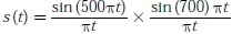 is given by
is given by
Answer : Option C
Explaination / Solution:
S(t) = sinc(500t) sinc(700t)
S(f ) is convolution of two signals whose spectrum covers f1 = 250 Hz and f2 = 350 Hz. So convolution extends
f = 25 + 350 = 600 Hz
Nyquist sampling rate
N = 2f = 2#600 = 1200 Hz
Q9. 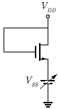
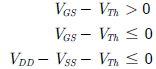
For the NMOSFET in the circuit shown, the threshold voltage is Vth, where Vth > 0. The source voltage VSS is varied from 0 to VDD. Neglecting the channel length modulation, the drain current ID as a function VSS is represented by
Answer : Option A
Explaination / Solution:
We have the following conditions
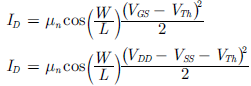
Since it is in saturation, current ID is given by
Thus, ID - VSS graph shows Parabolic relation for Vss < VDD
- Vth and zero for Vss > VDD
- Vth. Only graph shown in option (A) satisfies this result.
Q10. An 8085 assembly language program is given below.
Line 1: MVI A, B5H
2: MVI B, OEH
3: XRI 69H
4: ADD B
5: ANI 9BH
6: CPI 9FH
7: STA 3010H
8: HLT
The contents of the accumulator just execution of the ADD instruction in line 4 will be
Answer : Option B
Explaination / Solution:
Line 1 : MVI A, B5H ; Move B5H to A
2 : MVI B, 0EH ; Move 0EH to B
3 : XRI 69H ; [A] XOR 69H and store in A
; Contents of A is CDH
4 : ADDB ; Add the contents of A to contents of B and
; store in A, contents of A is EAH
5 : ANI 9BH ; [a] AND 9BH, and store in A,
; Contents of A is 8 AH
6 : CPI 9FH ; Compare 9FH with the contents of A
; Since 8 AH < 9BH, CY = 1
7 : STA 3010 H ; Store the contents of A to location 3010 H
8 : HLT ; Stop
Thus the contents of accumulator after execution of ADD instruction is EAH.
