Electrical Engineering - Online Test
Q1. Consider the two cascaded 2-to-1 multiplexers as shown in the figure.
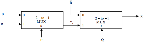
The minimal sum of products form of the output X is
Answer : Option D
Explaination / Solution:
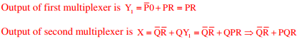
Q2. Three capacitors C1, C2, and C3, whose values are 10µF, 5µF, and 2µF respectively, have
breakdown voltages of 10V, 5V, and 2V respectively. For the interconnection shown, the maximum
safe voltage in Volts that can be applied across the combination and the corresponding total charge
in µC stored in the effective capacitance across the terminals are respectively
Answer : Option C
Explaination / Solution:
No Explaination.
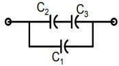
Q3. Two infinitely long wires carrying current are as shown in the figure below. One wire is in the y - z plane and parallel to the y axis. The other wire is in the x - y plane and parallel to the x - axis. Which components of the resultingmagnetic field are non-zero at the origin ?
Answer : Option D
Explaination / Solution:
Due to 1 A current wire in x - y plane, magnetic field be at origin will be in x direction.
Due to 1 A current wire in y - z plane, magnetic field be at origin will be in z direction.
Thus x and z component is non-zero at origin.
Due to 1 A current wire in y - z plane, magnetic field be at origin will be in z direction.
Thus x and z component is non-zero at origin.
Q4. The state transition matrix for the system
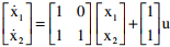 is
is
is
Answer : Option C
Explaination / Solution:
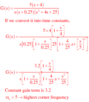
Q5. For the transfer function
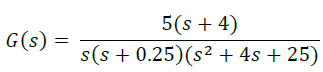
The values of the constant gain term and the highest corner frequency of the Bode plot respectively are
Answer : Option A
Explaination / Solution:
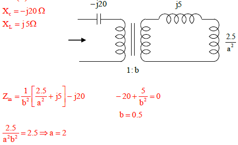
Q6. Find the transformer ratios a and b that the impedance (Zin) is resistive and equal
2.5Ω when the network is excited with a sine wave voltage of angular frequency of 5000 rad/s.
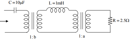
Answer : Option B
Explaination / Solution:
Q7. 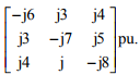
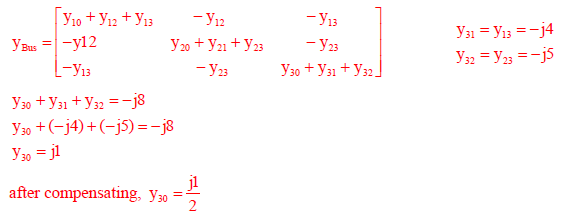
A 3-bus power system network consists of 3 transmission lines. The bus admittance matrix of the uncompensated system is
If the shunt capacitance of all transmission line is 50% compensated, the imaginary part
of the 3rd row 3rd column element (in pu) of the bus admittance matrix after compensation
is
Answer : Option B
Explaination / Solution:

Q8. The following discrete-time equations result from the numerical integration of the differential equations of an un-damped simple harmonic oscillator with state variables x and y. The integration time step is h.
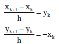
For this discrete-time system, which one of the following statements is TRUE?
Answer : Option A
Explaination / Solution:
No Explaination.
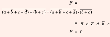
Q9. The Boolean expression 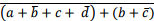 simplifies to
simplifies to
Answer : Option D
Explaination / Solution:
Q10. 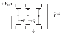
The logic function implemented by the following circuit at the terminal OUT is
Answer : Option D
Explaination / Solution:
From the figure shown below it may be easily seen upper MOSFET are shorted
and connected to Vdd thus OUT is 1 only when the node S is 0,
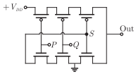
Since the lower MOSFETs are shorted to ground, node S is 0 only when input P
and Q are 1. This is the function of AND gate.
