Electronics Engineering - Online Test
Q1. The impulse response of a system is h(t) = tu(t). For an input u(t − 1), the output is
Answer : Option C
Explaination / Solution:
No Explaination.
Q2. Assuming the diodes to be ideal in the figure, for the output to be clipped, the input voltage vi must be outside the range
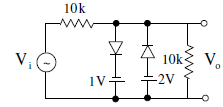
Answer : Option B
Explaination / Solution:
Q3. A binary operation ⊕ on a set of integers is defined as x ⊕ y = x2 + y2. Which one of the
following statements is TRUE about ⊕?
Answer : Option A
Explaination / Solution:
x ⊕ y = x2 + y2 = y2 + x2 = y ⊕ x
∴ commutative
Not associative, since, for example
(1 ⊕ 2) ⊕ 3 ≠ 1 ⊕ (2 ⊕ 3)
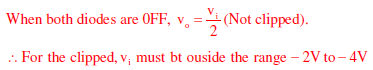
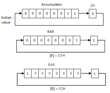
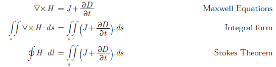
Q4.
In an 8085 microprocessor, the following program is executed
Address location – Instruction
2000H XRA A
2001H MVI B,04H
2003H MVI A, 03H
2005H RAR
2006H DCR B
2007H JNZ 2005
200AH HLT
At the end of program, register A contains
Answer : Option A
Explaination / Solution:
Q5. In a transconductance amplifier, it is desirable to have
Answer : Option A
Explaination / Solution:
In the transconductance amplifier it is desirable to have large input resistance and large output resistance.
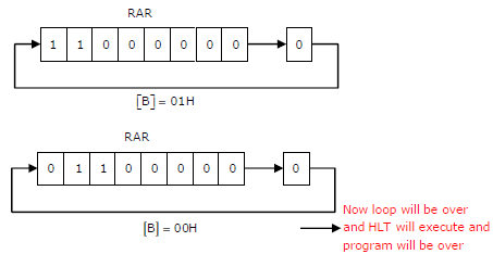
Q6. If C is code curve enclosing a surface S , then magnetic field intensity  , the
current density
, the
current density  and the electric flux density
  are related by
Answer : Option D
Explaination / Solution:
Q7. For the Op-Amp circuit shown in the figure, V is
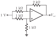
Answer : Option C
Explaination / Solution:
No Explaination.
Q8. Two 4-array signal constellations are shown. It is given that φ1 and φ2 constitute an orthonormal basis for the two constellation. Assume that the four symbols in both the constellations are equiprobable. Let N0/2 denote the power spectral density of white Gaussian noise.
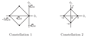
If these constellations are used for digital communications over an AWGN channel, then which of the following statements is true ?
Answer : Option A
Explaination / Solution:
No Explaination.
Q9.
The measured trans conductance gm of an NMOS transistor operating in the linear region is plotted against the gate voltage VG at a constant drain voltage VD. Which of the following figures represents the expected dependence of gm on VG ?
Answer : Option C
Explaination / Solution:
No Explaination.
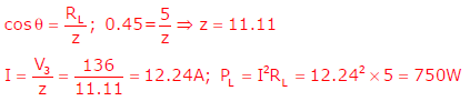
Q10. In the circuit shown, the three voltmeter readings are V1 = 220 V , V2 = 122 V, V3 = 136 V .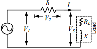
If RL = 5Ω , the approximate power consumption in the load is
Answer : Option B
Explaination / Solution: