Electronics Engineering - Online Test
Q1.
The figure shows the high-frequency capacitance - voltage characteristics of Metal/Sio2/silicon (MOS) capacitor having an area of 1 × 10⁻⁴ cm2. Assume that the permittivities (ε0εr) of silicon and Sio are 1 × 10-12 F/cm and 3.5 × 10⁻¹³ F/ cm respectively.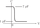
Consider the following statements about the C − V characteristics plot :
S1 : The MOS capacitor has as n-type substrate
S2 : If positive charges are introduced in the oxide, the C − V polt will shift to the left.
Then which of the following is true?
Answer : Option C
Explaination / Solution:
Depletion region will not be formed if the MOS capacitor has n type substrate but from C-V characteristics, C reduces if V is increased. Thus depletion region must be formed. Hence S1 is false
If positive charges is introduced in the oxide layer, then to equalize the effect the applied voltage V must be reduced. Thus the C − V plot moves to the left. Hence S2 is true.
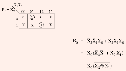
Q2. A 2-bit flash Analog to Digital Converter (ADC) is given below. The input is 0 ≤ VIN ≤ 3 Volts.
The expression for the LSB of the output B0 as a Boolean function of X2, X1, and X0 is
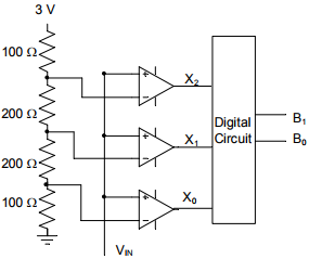
Answer : Option A
Explaination / Solution:
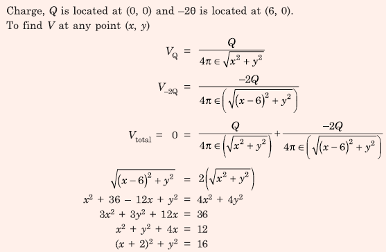
Q3. Two electric charges q and −2q are placed at (0,0) and (6,0) on the x-y plane. The equation of the zero equipotential curve in the x-y plane is
Answer : Option D
Explaination / Solution:
Q4. An RLC circuit with relevant data is given below.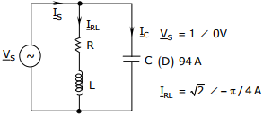
The power dissipated in the resistor R is
Answer : Option B
Explaination / Solution:
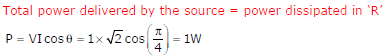
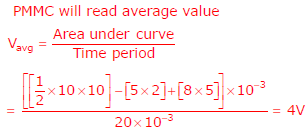
Q5. 
A periodic voltage waveform observed on an oscilloscope across a load is shown. A permanent magnet moving coil (PMMC) meter connected across the same load reads
Answer : Option A
Explaination / Solution:
Q6. The unilateral Laplace transform of f (t) is  . The unilateral Laplace transform of
t f (t)
is
. The unilateral Laplace transform of
t f (t)
is
. The unilateral Laplace transform of
t f (t)
is
Answer : Option D
Explaination / Solution:

Q7. In the 3-phase inverter circuit shown, the load is balanced and the gating scheme is 1800 -conduction mode.
All the switching devices are ideal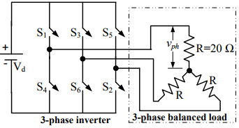
The rms value of load phase voltage is
Answer : Option B
Explaination / Solution:

Q8. Consider the following circuit involving three D-type flip-flops used in a certain type of counter configuration.
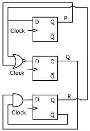
If at some instance prior to the occurrence of the clock edge, P. Q and R have a
value 0, 1 and 0 respectively, what shall be the value of PQR after the clock
edge?
Answer : Option D
Explaination / Solution:
From the Table Shown in the explanation of question 50, if first state is 010 next
State is 011
Q9. 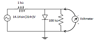
The input impedance of the permanent magnet moving coil (PMMC) voltmeter is infinite. Assuming that the diode shown in the figure below is ideal, the reading of the voltmeter in Volts is
Answer : Option A
Explaination / Solution:
No Explaination.
Q10. In the circuit shown below, Q1 has negligible collector-to-emitter saturation
voltage and the diode drops negligible voltage across it under forward bias. If Vcc is +5V, X and Y are digital signals with 0V as logic 0 and Voc as logic 1, then the
Boolean expression for Z is
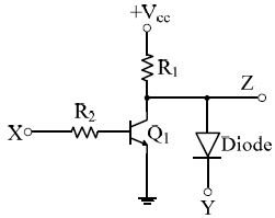
Answer : Option B
Explaination / Solution:
No Explaination.
