Electronic Science - Online Test
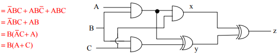
Q1. The output of the combinational circuit given below is

Answer : Option C
Explaination / Solution:

Q2. A network consisting of a finite number of linear resistor (R), inductor (L), and capacitor (C)
elements, connected all in series or all in parallel, is excited with a source of the form
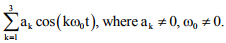
The source has nonzero impedance. Which one of the following is a possible form of the
output measured across a resistor in the network?
Answer : Option A
Explaination / Solution:
The property of any LTI system or network is if the excitation contains „n‟ number of different
frequency then the response also contains exactly n number of different frequency term and the
output frequency and input frequency must be same however depending on components there
is a possible change in amplitude and phase but never the frequency.
⟶ If the source has 3 frequency terms as given  then any voltage or any current of any element should have also 3 terms based on this option (B) and (D) are eliminated.
then any voltage or any current of any element should have also 3 terms based on this option (B) and (D) are eliminated.⟶ If we take option (C). It has 3 frequency term but it also suggest there is a phase change so ϕk but amplitude must be same as input as ak is present which may not be true always.
⟶ So option (A) is correct, as it suggest frequency term of output and inputs are same with
possible change in amplitude and phase, because we have (bk and ϕk ).
Q3. Identify the circuit below.
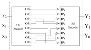
Answer : Option A
Explaination / Solution:
No Explaination.
Q4. The functionality implemented by the circuit below is
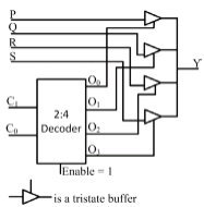
Answer : Option B
Explaination / Solution:
Decoder inputs will behaves as MUX select lines and when the output of decoder is high then only corresponding buffer will be enable and passed the inputs (P,Q,R,S) to the outpuut line, so it will work as 4-to-1 multiplexer.
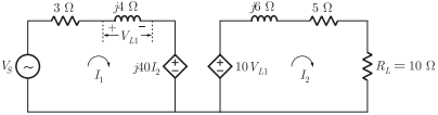
Q5. In the circuit shown below, if the source voltage  then the
Thevenin’s equivalent voltage in Volts as seen by the load resistance RL is
then the
Thevenin’s equivalent voltage in Volts as seen by the load resistance RL is
then the
Thevenin’s equivalent voltage in Volts as seen by the load resistance RL is
Answer : Option C
Explaination / Solution:
No Explaination.
Q6. In an 8085 system, a PUSH operation requires more clock cycles than a POP operation. Which one of the following options is the correct reason for this?
Answer : Option C
Explaination / Solution:
In push operation 3 cycles involved: 6T+3T+3T = 127
POP operation 3 cycle involved: 4T+3T+3T = 107
So in the opcode fetch cycle 2T states are extra in case of push compared to POP and this is needed to decrement the SP.
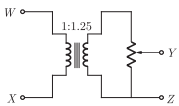
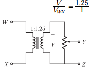
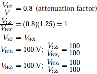
Q7. The following arrangement consists of an ideal transformer and an attenuator
which attenuates by a factor of 0.8. An ac voltage VWXI = 100 V is applied
across WX to get an open circuit voltage VYZ1 across YZ. Next, an ac voltage VYZ2 = 100 V is applied across YZ to get an open circuit voltage VWX2 across
WX. Then, VYZI/VWX1, VWX2/VYZ2 are respectively.
Answer : Option C
Explaination / Solution:
Q8. The DFT of a vector [a b c d] is the vector [α β γ δ]. Consider the product 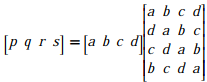
The DFT of the vector [p q r s] is a scaled version of
Answer : Option A
Explaination / Solution:
No Explaination.
Q9. A voltage 1000 sin𝜔t Volts is applied across YZ . Assuming ideal diodes, the
voltage measured across WX in Volts, is
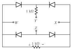
Answer : Option D
Explaination / Solution:
No Explaination.
Q10. In the circuit shown below, Q1 has negligible collector-to-emitter saturation voltage and the diode drops negligible voltage across it under forward bias. If Vcc is +5 V, X and Y are digital signals with 0 V as logic 0 and Vcc as logic 1,
then the Boolean expression for Z is
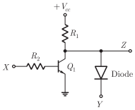
Answer : Option B
Explaination / Solution:
No Explaination.
