Electronics Engineering - Online Test
Q1. 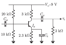
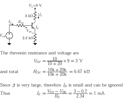
In the following transistor circuit, 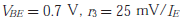 , and 𝛽 and all the capacitances are very large
, and 𝛽 and all the capacitances are very largeThe value of DC current IE is
Answer : Option A
Explaination / Solution:
For the given DC values the Thevenin equivalent circuit is as follows
Q2. A system with transfer function  has an output
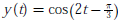 for the input signal
  Then, the system parameter p is
has an output for the input signal Then, the system parameter p is
Answer : Option B
Explaination / Solution:
Transfer function is given as
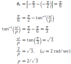
Amplitude Response
Alternative :
Q3. A small percentage of impurity is added to an intrinsic semiconductor at 300 K. Which one of
the following statements is true for the energy band diagram shown in the following figure?
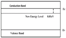
Answer : Option A
Explaination / Solution:
New energy level is near to conduction band, so it is pentavalent atoms to form n-type semiconductor.
Q4.
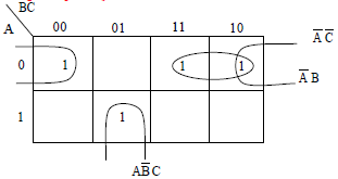
Which one of the following gives the simplified sum of products expression for the Boolean function F =
m0 + m2 + m3 + m5, where m0,
m2, m3
and m5 are minterms corresponding to the inputs A, B and C with A as the MSB and C as the LSB?
and m5 are minterms corresponding to the inputs A, B and C with A as the MSB and C as the LSB?
Answer : Option B
Explaination / Solution:
F =
m0 + m2 + m3 + m5, ⟶ minterm
Q5. In an 8085 microprocessor, the shift registers which store the result of an addition and the overflow bit are, respectively
Answer : Option B
Explaination / Solution:
The shift registers A and F store the result of an addition and the overflow bit.
Q6. The modes in a rectangular waveguide are denoted by  where
m n and are the eigen numbers along the larger and smaller dimensions of the
waveguide respectively. Which one of the following statements is TRUE?
where
m n and are the eigen numbers along the larger and smaller dimensions of the
waveguide respectively. Which one of the following statements is TRUE?
Answer : Option A
Explaination / Solution:
TM11 is the lowest order mode of all the TMmn modes
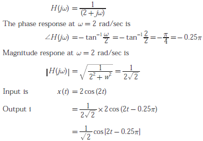
Q7. The impulse response h(t) of linear time - invariant continuous time system is given by h(t) = exp(- 2t)u(t), where u(t) denotes the unit step function.
The output of this system, to the sinusoidal input x(t) = 2 cos 2t for all time t , is
Answer : Option D
Explaination / Solution:
Q8. 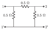
For the two-port network shown below, the short-circuit admittance parameter matrix is
Answer : Option A
Explaination / Solution:
Given circuit is as shown below
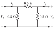
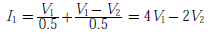
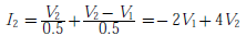
By writing node equation at input port
By writing node equation at output port
From (1) and (2), we have admittance matrix
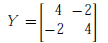
Q9. 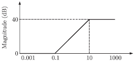
For the asymptotic Bode magnitude plot shown below, the system transfer function can be
Answer : Option A
Explaination / Solution:
Initial slope is zero, so K = 1
At corner frequency 𝜔1 = 0.5 rad/ sec, slope increases by +20 dB/decade, so there is a zero in the transfer function at 𝜔1
At corner frequency 𝜔2 = 10 rad/ sec, slope decreases by -20 dB/decade and becomes zero, so there is a pole in transfer function at 𝜔2
Transfer function 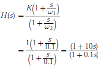
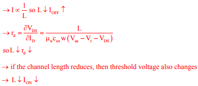
Q10. Consider the following statements for a metal oxide semiconductor field effect transistor
(MOSFET):
P: As channel length reduces, OFF-state current increases.
Q:As channel length reduces, output resistance increases.
R: As channel length reduces, threshold voltage remains constant.
S: As channel length reduces, ON current increases.
Which of the above statements are INCORRECT?
Answer : Option C
Explaination / Solution: