Analog and Digital Electronics - Online Test
Q1. An 8085 assembly language program is given below.
Line 1: MVI A, B5H
2: MVI B, OEH
3: XRI 69H
4: ADD B
5: ANI 9BH
6: CPI 9FH
7: STA 3010H
8: HLT
After execution of line 7 of the program, the status of the CY and Z flags will be
Answer : Option C
Explaination / Solution:
No Explaination.
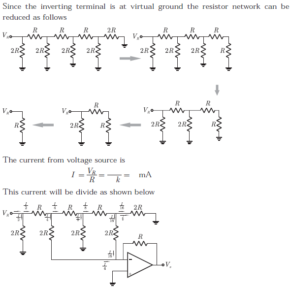
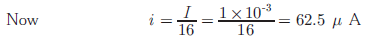
Q2. In the Digital-to-Analog converter circuit shown in the figure below, VR = 1V and R = 1kΩ
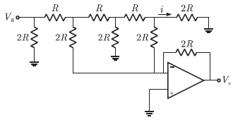
The current i is
Answer : Option B
Explaination / Solution:
Q3. An 8085 executes the following instructions
2710 LXI H, 30A0 H
2713 DAD H
2414 PCHL
All address and constants are in Hex. Let PC be the contents of the program counter and HL be the contents of the HL register pair just after executing PCHL. Which of the following statements is correct ?
Answer : Option C
Explaination / Solution:
2710H LXI H, 30A0H ; Load 16 bit data 30A0 in HL pair
2713H DAD H ; 6140H ⟶ HL
2714H PCHL ; Copy the contents 6140H of HL in PC
Thus after execution above instruction contests of PC and HL are same and that is 6140H
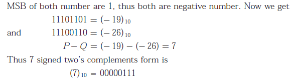
Q4. The two numbers represented in signed 2’s complement form are P + 11101101 and Q = 11100110. If Q is subtracted from P, the value obtained in signed 2’s complement is
Answer : Option B
Explaination / Solution:
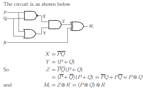
Q5. Which of the following Boolean Expressions correctly represents the relation
between P,Q,R and M1
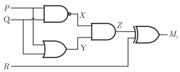
Answer : Option D
Explaination / Solution:
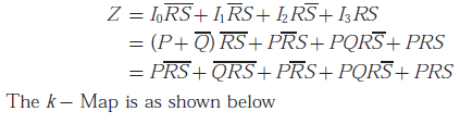
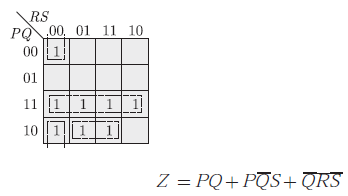
Q6. For the circuit shown in the following, I0 - I3 are inputs to the 4:1 multiplexers,
R(MSB) and S are control bits. 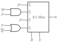
The output Z can be represented by
Answer : Option A
Explaination / Solution:
Q7. 
For each of the positive edge-triggered J - K flip flop used in the following figure, the propagation delay is Δt .
Which of the following wave forms correctly represents the output at Q1?
Answer : Option B
Explaination / Solution:
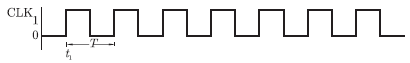
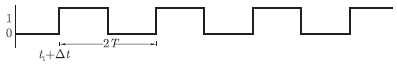
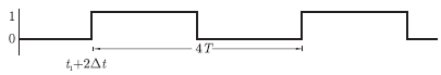
Since the input to both JK flip-flop is 11, the output will change every time with clock pulse. The input to clock is
The output Q0 of first FF occurs after time ΔT and it is as shown below
The output Q1 of second FF occurs after time ΔT when it gets input (i.e. after ΔT from t1) and it is as shown below
Q8. 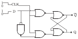
For the circuit shown in the figure, D has a transition from 0 to 1 after CLK changes from 1 to 0. Assume gate delays to be negligible. Which of the following statements is true
Answer : Option A
Explaination / Solution:
No Explaination.
Q9. 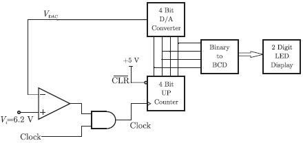
In the following circuit, the comparators output is logic “1” if V1 > V2 and is logic "0" otherwise. The D/A conversion is done as per the relation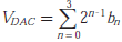 Volts, where b3 (MSB), b1,b2 and b0 (LSB) are the counter outputs. The counter starts from the clear state.
Volts, where b3 (MSB), b1,b2 and b0 (LSB) are the counter outputs. The counter starts from the clear state.The stable reading of the LED displays is
Answer : Option D
Explaination / Solution:
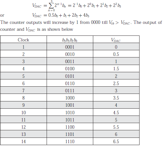
and when VADC = 6.5 V (at 1101), the output of AND is zero and the counter stops. The stable output of LED display is 13.
Q10.
In the following circuit, the comparators output is logic “1” if V1 > V2 and is logic "0" otherwise. The D/A conversion is done as per the relationVolts, where b3 (MSB), b1,b2 and b0 (LSB) are the counter outputs. The counter starts from the clear state.
Volts, where b3 (MSB), b1,b2 and b0 (LSB) are the counter outputs. The counter starts from the clear state.The magnitude of the error between VDAC and Vin at steady state in volts is
Answer : Option B
Explaination / Solution:
No Explaination.
