Analog and Digital Electronics - Online Test
Q1. Consider the oscillator circuit shown in the figure. The function of the network (shown in
dotted lines) consisting of the
100kΩ resistor in series with the two diodes connected back-toback
is to:
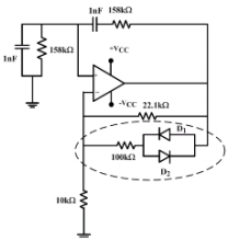
Answer : Option A
Explaination / Solution:
When the output voltage is positive the diode D1 is turned on making 100kΩ resistor to become parallel to 22.1kΩ. So the gain is reduced. When the output voltage becomes negative the diode D2 is turned on thereby again 100kΩ resistor to become parallel to 22.1kΩ. So the gain is reduced. With the use of diodes, the non ideal OP-Amp is made stable to produce steady
Q2. The Boolean function Y = AB + CD is to be realized using only 2 - input NAND gates. The minimum number of gates required is
Answer : Option B
Explaination / Solution:
This is SOP form and we require only 3 NAND gate
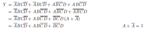
Q3. The Boolean expression  can be
minimized to
can be
minimized to
can be
minimized to
Answer : Option D
Explaination / Solution:
Q4. In the circuit shown below the op-amps are ideal. Then, Vout in Volts is
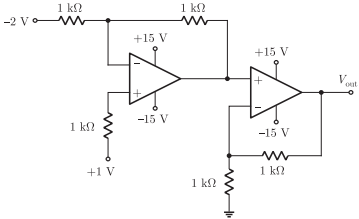
Answer : Option C
Explaination / Solution:
No Explaination.
Q5. The circuit diagram of a standard TTL NOT gate is shown in the figure. Vi = 25 V, the modes of operation of the transistors will be
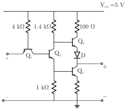
Answer : Option B
Explaination / Solution:
No Explaination.
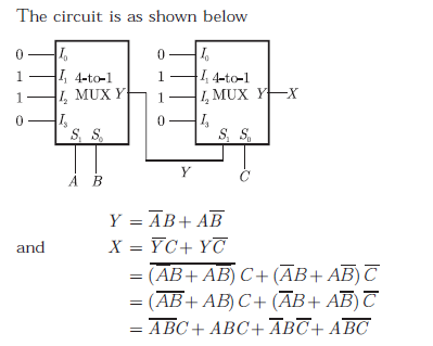
Q6. In the following circuit, X is given by
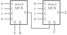
Answer : Option A
Explaination / Solution:
Q7. The following binary values were applied to the X and Y inputs of NAND latch
shown in the figure in the sequence indicated below : 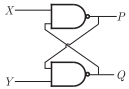
X = ,Y = X = ,Y = X = Y =
The corresponding stable P Q, output will be
Answer : Option C
Explaination / Solution:
No Explaination.
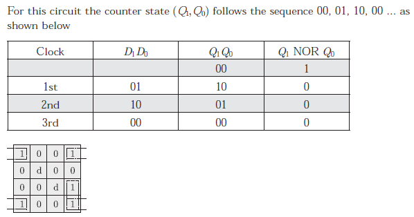
Q8. For the circuit shown, the counter state (Q1Q0) follows the sequence
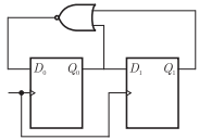
Answer : Option A
Explaination / Solution:
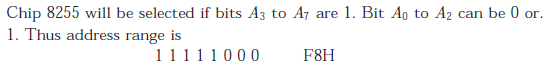
Q9. An 8255 chip is interfaced to an 8085 microprocessor system as an I/O mapped
I/O as show in the figure. The address lines A0 and A1 of the 8085 are used
by the 8255 chip to decode internally its thee ports and the Control register.
The address lines A3 to A as well as the  signal are used for address
decoding. The range of addresses for which the 8255 chip would get selected is
signal are used for address
decoding. The range of addresses for which the 8255 chip would get selected is
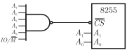
Answer : Option C
Explaination / Solution:
Q10. An 8085 assembly language program is given below.
Line 1: MVI A, B5H
2: MVI B, OEH
3: XRI 69H
4: ADD B
5: ANI 9BH
6: CPI 9FH
7: STA 3010H
8: HLT
The contents of the accumulator just execution of the ADD instruction in line 4 will be
Answer : Option B
Explaination / Solution:
Line 1 : MVI A, B5H ; Move B5H to A
2 : MVI B, 0EH ; Move 0EH to B
3 : XRI 69H ; [A] XOR 69H and store in A
; Contents of A is CDH
4 : ADDB ; Add the contents of A to contents of B and
; store in A, contents of A is EAH
5 : ANI 9BH ; [a] AND 9BH, and store in A,
; Contents of A is 8 AH
6 : CPI 9FH ; Compare 9FH with the contents of A
; Since 8 AH < 9BH, CY = 1
7 : STA 3010 H ; Store the contents of A to location 3010 H
8 : HLT ; Stop
Thus the contents of accumulator after execution of ADD instruction is EAH.
