Electronic Devices - Online Test
Q1. Which of the following is true?
Answer : Option A
Explaination / Solution:
Trivalent impurities are used for making p - type semiconductors. So, Silicon wafer heavily doped with boron is a p+ substrate.
Q2. In the following limiter circuit, an input voltage Vi = 10 sin100πt is applied.
Assume that the diode drop is 0.7 V when it is forward biased. When it is
forward biased. The zener breakdown voltage is 6.8 V
The maximum and minimum values of the output voltage respectively are
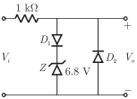
Answer : Option C
Explaination / Solution:
No Explaination.
Q3. A silicon wafer has 100 nm of oxide on it and is furnace at a temperature above
10000 C for further oxidation in dry oxygen. The oxidation rate
Answer : Option D
Explaination / Solution:
No Explaination.
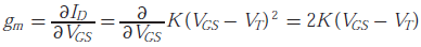
Q4. The drain current of MOSFET in saturation is given by 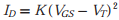 where K is a constant.
where K is a constant. The magnitude of the transconductance gm is
Answer : Option B
Explaination / Solution:
Q5. 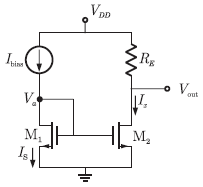
For the circuit shown in the following figure, transistor M1 and M2 are identical NMOS transistors. Assume the M2 is in saturation and the output is unloaded.
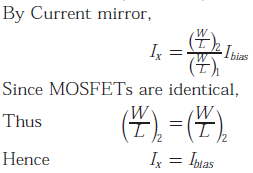
The current Ix is related to Ibias as
Answer : Option B
Explaination / Solution:
Q6.
The measured trans conductance gm of an NMOS transistor operating in the linear region is plotted against the gate voltage VG at a constant drain voltage VD. Which of the following figures represents the expected dependence of gm on VG ?
Answer : Option C
Explaination / Solution:
No Explaination.
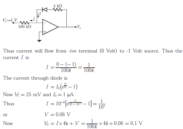
Q7. Consider the following circuit using an ideal OPAMP. The I-V characteristic of
the diode is described by the relation  where VT = 25 mV, I0 = 1μ A and V is the voltage across the diode (taken as positive for forward bias). For
an input voltage Vi = -1 V, the output voltage V0 is
where VT = 25 mV, I0 = 1μ A and V is the voltage across the diode (taken as positive for forward bias). For
an input voltage Vi = -1 V, the output voltage V0 is
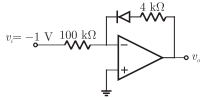
where VT = 25 mV, I0 = 1μ A and V is the voltage across the diode (taken as positive for forward bias). For
an input voltage Vi = -1 V, the output voltage V0 is
Answer : Option B
Explaination / Solution:
Q8. 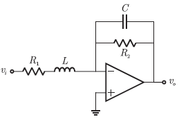
The OPAMP circuit shown above represents a
Answer : Option B
Explaination / Solution:
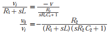
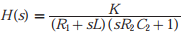
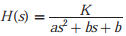
and from this equation it may be easily seen that this is the standard form of
T.F. of low pass filter
and form this equation it may be easily seen that this is the standard form of
T.F. of low pass filter
Q9. Two identical NMOS transistors M1 and M2 are connected as shown below.
Vbias is chosen so that both transistors are in saturation. The equivalent gm of
the pair is defied to be  at constant Vout
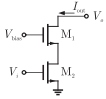
The equivalent gm of the pair is
Answer : Option C
Explaination / Solution:
No Explaination.
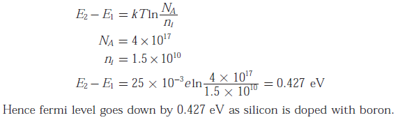
Q10. Silicon is doped with boron to a concentration of 4 × 10¹⁷ atoms cm3. Assume
the intrinsic carrier concentration of silicon to be 1.5 × 10¹⁰/cm3 and the value
of kT/q to be 25 mV at 300 K. Compared to undopped silicon, the fermi level
of doped silicon
Answer : Option C
Explaination / Solution: