Analog and Digital Electronics - Online Test
Q1. The output of a 3-stage Johnson (twisted ring) counter is fed to a digital-to
analog (D/A) converter as shown in the figure below. Assume all the states
of the counter to be unset initially. The waveform which represents the D/A
converter output v0 is

Answer : Option A
Explaination / Solution:
All the states of the counter are initially unset.

State Initially are shown below in table:
Q2Q1Q0
0 0 0 0
1 0 0 4
1 1 0 6
1 1 1 7
0 1 1 3
0 0 1 1
0 0 0 0
Q2. Two D flip-flops are connected as a synchronous counter that goes through the
following QBQA sequence 00⟶11⟶01⟶10⟶00⟶… The combination to the inputs DA and DB are
Answer : Option D
Explaination / Solution:
The sequence is QBQA
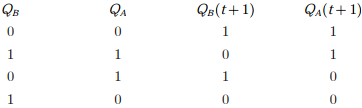
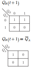

00⟶11⟶01⟶10⟶00⟶…
Q3. An 8085 assembly language program is given below. Assume that the carry
flag is initially unset. The content of the accumulator after the execution of the
program is
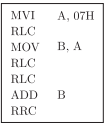
Answer : Option C
Explaination / Solution:
Initially Carry Flag, C = 0
MVI A, 07 H ; A = 0000 0111
RLC ; Rotate left without carry. A = 00001110
MVO B, A ; B = A = 00001110
RLC ; A = 00011100
RLC ; A = 00111000
ADD B ; A = 00111000
; +00001110
; 01000110
RRC ; Rotate Right with out carry, A = 0010 0011
Thus A = 23 H
Q4. The first six points of the 8-point DFT of a real valued sequence are 5, 1 - j3, 0, 3 - 4j, 0 and 3 + 4j .....The last two points of the DFT are respectively
Answer : Option B
Explaination / Solution:
For 8 point DFT,  and it is conjugate
symmetric about x[4], x[6] = 0; x[7] = 1 + j3
and it is conjugate
symmetric about x[4], x[6] = 0; x[7] = 1 + j3
and it is conjugate
symmetric about x[4], x[6] = 0; x[7] = 1 + j3
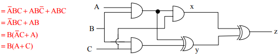
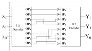
Q5. The output of the combinational circuit given below is

Answer : Option C
Explaination / Solution:

Q6. Identify the circuit below.
Answer : Option A
Explaination / Solution:
No Explaination.
Q7. The functionality implemented by the circuit below is
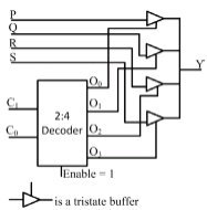
Answer : Option B
Explaination / Solution:
Decoder inputs will behaves as MUX select lines and when the output of decoder is high then only corresponding buffer will be enable and passed the inputs (P,Q,R,S) to the outpuut line, so it will work as 4-to-1 multiplexer.
Q8. In an 8085 system, a PUSH operation requires more clock cycles than a POP operation. Which one of the following options is the correct reason for this?
Answer : Option C
Explaination / Solution:
In push operation 3 cycles involved: 6T+3T+3T = 127
POP operation 3 cycle involved: 4T+3T+3T = 107
So in the opcode fetch cycle 2T states are extra in case of push compared to POP and this is needed to decrement the SP.
Q9. The DFT of a vector [a b c d] is the vector [α β γ δ]. Consider the product 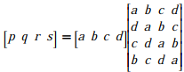
The DFT of the vector [p q r s] is a scaled version of
Answer : Option A
Explaination / Solution:
No Explaination.
Q10. In the circuit shown below, Q1 has negligible collector-to-emitter saturation voltage and the diode drops negligible voltage across it under forward bias. If Vcc is +5 V, X and Y are digital signals with 0 V as logic 0 and Vcc as logic 1,
then the Boolean expression for Z is
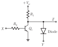
Answer : Option B
Explaination / Solution:
No Explaination.
