Electronic Devices - Online Test
Biasing is the application of a voltage across a p–n junction.
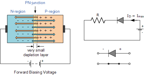
When we connect p-type region of a junction with the positive terminal of a voltage source and n-type region with the negative terminal of the voltage source, then the junction is said to be forward biased.
At this condition, due to the attraction of positive terminal of source, electrons which participated in covalent bond creations in p-type material, will be attracted towards the terminal.
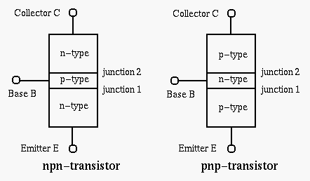
A transistor consisting of two p-n junctions combined to form either an n-p-n or a p-n-p transistor, having the three electrodes, the emitter, base, and collector
A transistor is an electronic component that can be used as an amplifier, or as a switch. It is made of semiconductor material. Transistors are found in most electronic devices. 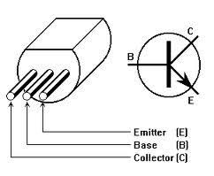
A transistor has three connectors or terminals. In the older bipolar transistor they are the collector, the emitter, and the base. The flow of charge goes in the collector, and out of the emitter, depending on the charge flowing to the base
When the p-type crystal is grown between relatively wide sections of n-type crystals then the transistor is called NPN transistor.
Current gain of transistor
Amplifier is an electronic device. The device which increases the value of a signal is called amplifier. In input a weak signal is applied, in output a strong, same shape signal is gained. Amplify means to increase the value of something.
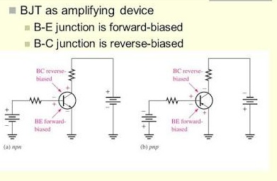
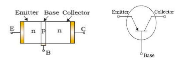
The collector is reverse biased and the emitter is forward biased while using transistor as an amplifier.
When a diode is connected in a Reverse Bias condition, a positive voltage is applied to the N-type material and a negative voltage is applied to the P-type material.
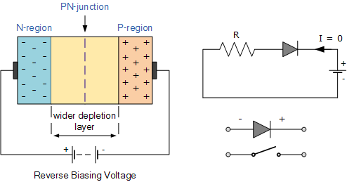
The positive voltage applied to the N-type material attracts electrons towards the positive electrode and away from the junction, while the holes in the P-type end are also attracted away from the junction towards the negative electrode.
The net result is that the depletion layer grows wider due to a lack of electrons and holes and presents a high impedance path, almost an insulator. The result is that a high potential barrier is created thus preventing current from flowing through the semiconductor material
