Electronic Devices - Online Test
The number of carriers in the conduction and valence band with no externally applied bias is called the equilibrium carrier concentration.
For majority carriers, the equilibrium carrier concentration is equal to the intrinsic carrier concentration plus the number of free carriers added by doping the semiconductor. Under most conditions, the doping of the semiconductor is several orders of magnitude greater than the intrinsic carrier concentration, such that the number of majority carriers is approximately equal to the doping.
At equilibrium, the product of the majority and minority carrier concentration is a constant, and this is mathematically expressed by the Law of Mass Action.
Where ni is the intrinsic carrier concentration and neand ph are the electron and hole equilibrium carrier concentrations.
- In n-type semiconductor, the concentration of electrons is more compared to the concentration of holes. Similarly, in p-type semiconductor, the concentration of holes is more compared to the concentration of electrons
- The first process that occurs in the p-n semiconductor is diffusion
- In the formation of the p-n junction, due to the concentration gradient across the p and the n sides, the electrons diffuse from n region to p region and the holes diffuse from p region to n region.
The material which has electrical conductivity between that of a conductor and an insulator is called as semiconductor. Silicon, germanium and graphite are some examples of semiconductors.
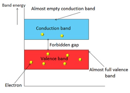
In semiconductors, the forbidden gap between valence band and conduction band is very small. It has a forbidden gap of about 1 electron volt (eV).
Forbidden gap plays a major role for determining the electrical conductivity of material. Based on the forbidden gap materials are classified in to three types, they are :
- Insulators : The forbidden gap between the valence band and conduction band is very large in insulators. The energy gap of insulator is approximately equal to 15 electron volts (eV).
- Conductors: In a conductor, valence band and conduction band overlap each other. Therefore, there is no forbidden gap in a conductor.
- Semiconductors: In semiconductors, the forbidden gap between valence band and conduction band is very small. It has a forbidden gap of about 1 electron volt (eV).
