EC GATE 2010 - Online Test
Q1. 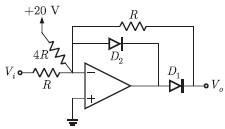
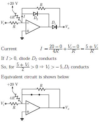
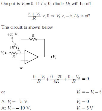
The transfer characteristic for the precision rectifier circuit shown below is (assume ideal OP-AMP and practical diodes)
Answer : Option B
Explaination / Solution:
Q2. 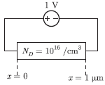
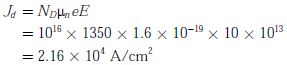
The silicon sample with unit cross-sectional area shown below is in thermal equilibrium. The following information is given: T = 300 K electronic charge = 1.6 × 10⁻¹⁹ C, thermal voltage = 26 mV and electron mobility = 1350 cm2 / V-s
The magnitude of the electron of the electron drift current density at x = 0.5 μm is
Answer : Option A
Explaination / Solution:
Electron drift current density
Q3. 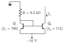
In the silicon BJT circuit shown below, assume that the emitter area of transistor Q1 is half that of transistor Q2
The value of current I0 is approximately
Answer : Option B
Explaination / Solution:
Since, emitter area of transistor Q1 is half of transistor Q2, so current
Q4. 

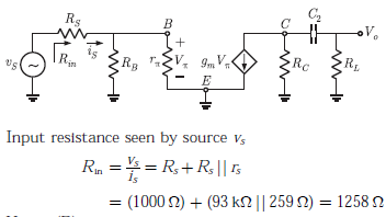
Consider the common emitter amplifier shown below with the following circuit parameters:
The resistance seen by the source vs is
Answer : Option B
Explaination / Solution:
Q5. 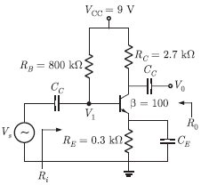
The amplifier circuit shown below uses a silicon transistor. The capacitors Cc and CE can be assumed to be short at signal frequency and effect of output resistance r0 can be ignored. If CE is disconnected from the circuit, which one of the following statements is true
Answer : Option A
Explaination / Solution:
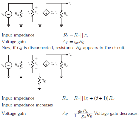
The equivalent circuit of given amplifier circuit (when CE is connected, RE is short-circuited)
Q6.
For a N -point FET algorithm N = 2m which one of the following statements is TRUE ?
Answer : Option D
Explaination / Solution:
For an N-point FET algorithm butterfly operates on one pair of samples and involves two complex addition and one complex multiplication.
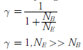
Q7.
In a uniformly doped BJT, assume that NE, NB and NC are the emitter, base and collector doping in atoms/cm3, respectively. If the emitter injection efficiency of the BJT is close unity, which one of the following condition is TRUE
Answer : Option B
Explaination / Solution:
Emitter injection efficiency is given as
Q8.
Compared to a p-n junction with NA = ND = 10-14/cm3, which one of the following statements is TRUE for a p-n junction with NA = ND = 10-20/cm3?
Answer : Option C
Explaination / Solution:
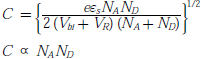
Reverse bias breakdown or Zener effect occurs in highly doped PN junction through tunneling mechanism. In a highly doped PN junction, the conduction and valence bands on opposite sides of the junction are sufficiently close during reverse bias that electron may tunnel directly from the valence band on the p-side into the conduction band on n-side.
Breakdown voltage 
So, breakdown voltage decreases as concentration increases
Depletion capacitance
Depletion capacitance increases as concentration increases
Q9. 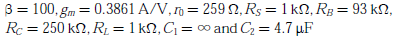
Consider the common emitter amplifier shown below with the following circuit parameters:
The lower cut-off frequency due to C2 is
Answer : Option B
Explaination / Solution:
Cut-off frequency due to C2
Lower cut-off frequency
Q10. 25 persons are in a room, 15 of them play hockey, 17 of them football and 10 of them play both hockey and football. Then the number of persons playing neither hockey nor football is ;
Answer : Option D
Explaination / Solution:
Number of people who play hockey n(A) = 15
Number of people who play football n(B) = 17
Persons who play both hockey and football n(A∩B) = 10
Persons who play either hockey or football or both :
n(AUB) = n(A) + n(B) - n(A∩B)
= 15 + 17 - 10 = 22
Thus people who play neither hockey nor football = 25 - 22 = 3
