EC GATE 2008 - Online Test
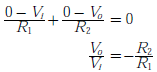
Q1. The cross section of a JFET is shown in the following figure. Let Vc be -2
V and let VP be the initial pinch -off voltage. If the width W is doubled (with
other geometrical parameters and doping levels remaining the same), then the
ratio between the mutual trans conductances of the initial and the modified
JFET is
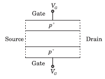
Answer : Option C
Explaination / Solution:
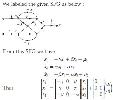
Q2. A signal flow graph of a system is given below
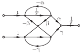
The set of equalities that corresponds to this signal flow graph is
Answer : Option C
Explaination / Solution:
Q3. Consider the Schmidt trigger circuit shown below
A triangular wave which goes from -12 to 12 V is applied to the inverting input
of OPMAP. Assume that the output of the OPAMP swings from +15 V to -15 V.
The voltage at the non-inverting input switches between
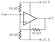
Answer : Option C
Explaination / Solution:
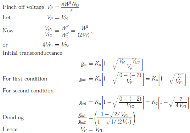
Let the voltage at non inverting terminal be V1, then after applying KCL at non
inverting terminal side we have
If V0 swings from -15 to +15 V then V1 swings between -5 V to +5 V.
Q4. Consider the following assertions.
S1 : For Zener effect to occur, a very abrupt junction is required.
S2 : For quantum tunneling to occur, a very narrow energy barrier is required.
Which of the following is correct ?
Answer : Option A
Explaination / Solution:
No Explaination.
Q5. 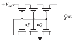
The logic function implemented by the following circuit at the terminal OUT is
Answer : Option D
Explaination / Solution:
From the figure shown below it may be easily seen upper MOSFET are shorted
and connected to Vdd thus OUT is 1 only when the node S is 0,
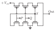
Since the lower MOSFETs are shorted to ground, node S is 0 only when input P
and Q are 1. This is the function of AND gate.
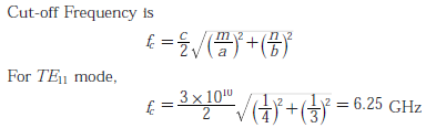
Q6.
A rectangular waveguide of internal dimensions (a = 4 cm and b = 3 cm) is to be operated in TE11 mode. The minimum operating frequency is
Answer : Option A
Explaination / Solution:
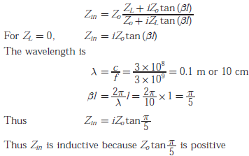
Q7. One end of a loss-less transmission line having the characteristic impedance of 75Ω and length of 1 cm is short-circuited. At 3 GHz, the input impedance at the other end of transmission line is
Answer : Option D
Explaination / Solution:
Q8. 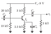
In the following transistor circuit, 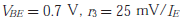 , and 𝛽 and all the capacitances are very large
, and 𝛽 and all the capacitances are very largeThe mid-band voltage gain of the amplifier is approximately
Answer : Option D
Explaination / Solution:
The small signal model is shown in fig below
Q9. In the design of a single mode step index optical fibre close to upper cut-off, the single-mode operation is not preserved if
Answer : Option C
Explaination / Solution:
No Explaination.
Q10. 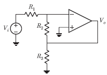
Assuming the OP-AMP to be ideal, the voltage gain of the amplifier shown below is
Answer : Option A
Explaination / Solution: