Electronic Devices - Online Test
Q1. The cross section of a JFET is shown in the following figure. Let Vc be -2
V and let VP be the initial pinch -off voltage. If the width W is doubled (with
other geometrical parameters and doping levels remaining the same), then the
ratio between the mutual trans conductances of the initial and the modified
JFET is
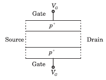
Answer : Option C
Explaination / Solution:
Q2. Consider the following assertions.
S1 : For Zener effect to occur, a very abrupt junction is required.
S2 : For quantum tunneling to occur, a very narrow energy barrier is required.
Which of the following is correct ?
Answer : Option A
Explaination / Solution:
No Explaination.
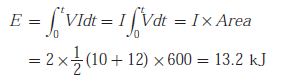
Q3. A fully charged mobile phone with a 12 V battery is good for a 10 minute talktime. Assume that, during the talk-time the battery delivers a constant current of 2 A and its voltage drops linearly from 12 V to 10 V as shown in the figure. How much energy does the battery deliver during this talk-time?
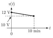
Answer : Option C
Explaination / Solution:
The energy delivered in 10 minutes is
Q4. The full form of the abbreviations TTL and CMOS in reference to logic families are
Answer : Option C
Explaination / Solution:
TTL -> Transistor - Transistor logic
CMOS -> Complementary Metal Oxide Semi-conductor
Q5. At room temperature, a possible value for the mobility of electrons in the inversion layer of a silicon n-channel MOSFET is
Answer : Option A
Explaination / Solution:
At room temperature mobility of electrons for Si sample is given μn = 1350 cm2/V-s For an n-channel MOSFET to create an inversion layer of electrons, a large positive gate voltage is to be applied. Therefore, induced electric field increases and mobility decreases.
So, Mobility μn <1350 cm2/V-s for n-channel MOSFET
Q6. Thin gate oxide in a CMOS process in preferably grown using
Answer : Option B
Explaination / Solution:
Dry oxidation is used to achieve high quality oxide growth.
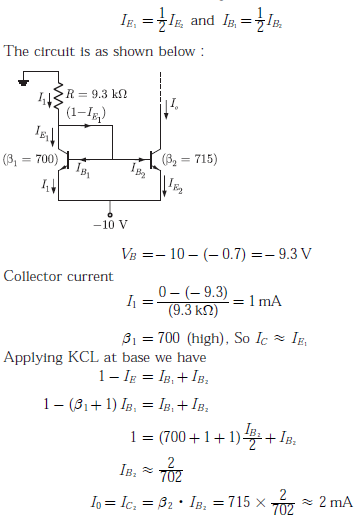
Q7. 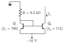
In the silicon BJT circuit shown below, assume that the emitter area of transistor Q1 is half that of transistor Q2
The value of current I0 is approximately
Answer : Option B
Explaination / Solution:
Since, emitter area of transistor Q1 is half of transistor Q2, so current
Q8. 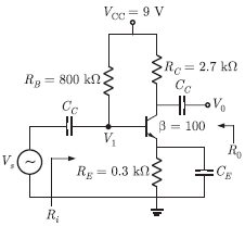
The amplifier circuit shown below uses a silicon transistor. The capacitors Cc and CE can be assumed to be short at signal frequency and effect of output resistance r0 can be ignored. If CE is disconnected from the circuit, which one of the following statements is true
Answer : Option A
Explaination / Solution:
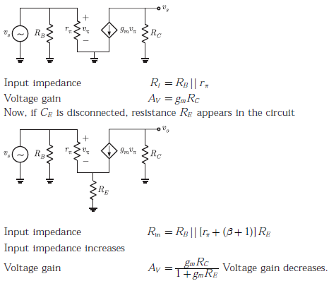
The equivalent circuit of given amplifier circuit (when CE is connected, RE is short-circuited)
Q9.
For a N -point FET algorithm N = 2m which one of the following statements is TRUE ?
Answer : Option D
Explaination / Solution:
For an N-point FET algorithm butterfly operates on one pair of samples and involves two complex addition and one complex multiplication.
Q10.
In a uniformly doped BJT, assume that NE, NB and NC are the emitter, base and collector doping in atoms/cm3, respectively. If the emitter injection efficiency of the BJT is close unity, which one of the following condition is TRUE
Answer : Option B
Explaination / Solution:
Emitter injection efficiency is given as